Plasmas can offer more than just etching straight down. This blog post aims to show that the etching community can benefit greatly from using plasmas for new applications. Currently, in the atomic layer etching (ALE) community plasmas are often considered only for anisotropic etching. In our recent work, which you can read or alternatively watch at the bottom of this blog, we used plasmas to achieve isotropic ALE, a process previously thought to be the domain of thermal reactions. Our aim was to develop an isotropic plasma ALE process to enable the complex geometries required for advanced IC designs, while also delivering some of the expected benefits of a plasma process.
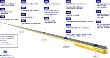
Before moving onto why we think plasma isotropic ALE will be a valuable addition to the ALE toolbox, we should first briefly discuss the field of ALE (a more in-depth history can be found here or here). The idea of using a plasma for ALE was not a new one. The first reported ALE process, a patent filed back in 1988, involves “removing a single atomic layer of crystalline diamond” by alternating between exposure of the surface to nitrogen dioxide and bombardment with noble gas ions from a plasma. [1] This controlled directional removal of material using a repeating two-step process laid the foundations for future ALE research. As directional species were used to remove the modified material, this kind of etching became known as anisotropic ALE. Unfortunately, at its inception there was no real demand for such a precise etching technique, which resulted in little following within academia or industry.

Despite the slow beginnings, anisotropic ALE has received a resurgence of interest in recent years. With industry striving towards ever smaller technology nodes to produce faster and smaller electronics, the demands for controlled and accurate processing techniques in IC fabrication have increased. [2] This demand has injected new life into the field of anisotropic ALE, boosting the number of publications per year from 25 in 2004 to over 250 per year in 2020. Several benefits such as high selectivity and smooth films after etching have been observed for anisotropic ALE over conventional etch processes. [3]
Being able to etch directionally is only half the picture. Isotropic processing is also required to fully realise the complex 3D structures desired in advanced IC devices. This can be seen by looking at GAAFET structures: anisotropic etching will be necessary to etch the fins while isotropic etching will be needed to produce the horizontal nanowires.[4] In 2015 while working toward thermal ALD of metal fluorides, the George group in Colorado discovered thermal ALE.[5] They showed that reactants used for thermal ALD could, when dosed in the correct conditions, also lead to ALE. The ability to transition between ALD and ALE by tuning the process parameters highlights how these atomic scale processing techniques can learn from each other. [6] As no directional species are used in either half-cycle, the material was removed independent of surface orientation. Since this first paper in 2015 there has been great interest in thermal ALE as shown by the rapid increase in papers published per year.
This is where our work comes in. Using ALD for inspiration, we tried to identify areas of ALE where plasmas could be used to bring process benefits. We saw the largely unexplored option of plasma isotropic ALE (the top right quadrant in the first figure) as a way to achieve isotropic etching while also exploiting possible benefits such as higher etch rates and lower operating temperatures. The thinking being if plasmas can be used for isotropic deposition in ALD, why not also for isotropic removal? Isotropic processing using plasmas is possible because when a plasma is ignited radicals are produced as well as ions and electrons. In plasma anisotropic ALE directional ions are desired, whereas in plasma isotropic ALE we instead exploit the radicals. Plasma radicals are neutral species and do not become directional in the plasma sheath, instead they diffuse towards the substrate like thermal reactants. Plasma radicals are also more reactive than thermal reactants, which, as the figure below shows, results in a lower activation barrier. This higher reactivity can translate into lower operating temperatures, higher etch rates and the potential to etch materials previously thought to be resistant to thermal ALE.

In our work we showed that an SF6 plasma and trimethylaluminium could be used to isotropically etch Al2O3, as can be seen in the cover image of this post. [8] If you would like to see more of the work you can read our recent publication here or watch the video at the bottom of the blog post. This is a recording of the presentation I gave at the ALD/ALE conference 2020 where I discuss our work, for which I was awarded the ‘Best ALE student paper’ award. Isotropic plasma ALE stands to bring many benefits to atomic scale processing, and I look forward to further investigating what can be made possible by utilizing plasmas.
References
- M. N. Yoder, US Pat. 4,756,794 A (1988).
- K. J. Kanarik, et al JVSTA: Vacuum, Surfaces, and Films, 33(2), p.020802 (2015)
- T. Ohba et al, Jpn. J. Appl. Phys. 56 06HB06 (2017)
- Semiengineering – “Atomic layer etch expands to new markets” https://semiengineering.com/atomic-layer-etch-expands-to-new-markets/
- Y. Lee, S. M. George, ACS Nano;9(2):2061-70. (2015)
- T. Faraz et al. ECS Journal of Solid State Science and Technology,4(6) N5023-N5032 (2015)
- J. Chang and J. P. Chang, J. Phys. D: Appl. Phys. 50 253001. (2017)
- N. J. Chittock, et al Applied Physics Letters, 117, 162107 (2020)
Images of ALE publications per year can be found in the image library.


Leave a Reply