This post is about the value of industry-academia partnerships, and about how such collaborations can trigger new innovations. This month exactly 3 years ago, we were approached by Prodrive Technologies, a company in the Eindhoven area developing and manufacturing electronics and mechatronics, to talk about the possibilities for developing a power supply for the plasma etch industry. We decided together to focus on tailored waveform biasing, a technology that saw the light about two decades ago,1 but was perhaps ahead of its time, and has not been adopted in the semiconductor industry yet. However, we believe that with the upcoming of atomic layer etching (ALE) and the need for atomic-scale processing in general, the time is ripe for this technology. In the meantime, there also has been a lot of development in power electronics, which opened up new possibilities for the design of a dedicated power supply enabling tailored waveform biasing.
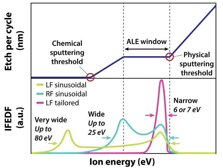
But why is tailored waveform biasing of interest for the ALE community? Although the ion energy is the most important parameter in anisotropic ALE, conventional radio frequency (RF) and low frequency (LF) sinusoidal bias waveforms result in relatively broad ion energy distributions, as illustrated in Figure 1. When applying substrate biasing with a specific tailored waveform, a narrow ion distribution can be obtained. In other words, tailored waveform biasing allows for processing using ions with a well-defined energy. The animation below illustrates the main concepts of tailored waveform biasing.

Tailored waveform biasing was originally developed in seminal work by Wendt and co-workers in the early 2000s.1 The current work also builds on earlier studies in our research group 10-15 years ago,2–4 in which it was applied for anisotropic etching of Si,2 and also for the deposition of hydrogenated amorphous Si.4,5 More information about tailored waveform biasing can also be found in the review paper by Economou.6
In our recent publication in the Journal of Applied Physics,7 we describe our first results obtained by implementing Prodrive’s prototype on an Oxford Instrument FlexAL reactor. We report on narrow ion energy distributions (7 ± 1 eV FWHM, i.e. comparably to the unbiased case) for ion energies between 0 and 200 eV, as shown in Figure 2. The control of the ion energy was shown to be independent of the ion flux. To demonstrate the use of tailored waveform for anisotropic etching, these mono-energic ions were subsequently employed to sputter etch SiO2 films. Those sputter etch experiments also illustrate an additional application for this technology: the control of the ion energy allows for accurate determination of sputter yields and threshold energies for ion energies < 100 eV. This type of data is at the moment only scarcely available in the literature, while it is essential input for the development of selective ALE processes (see Figure 1). The next step for our research will be to explore the opportunities for ALE. We expect that tailored waveform biasing will lead to anisotropic ALE processes with improved selectivity and reduced surface damage. The accurate control of the ion energy for example potentially allows for exploiting small differences in threshold energies to obtain selectivity.

Back to the topic of industry-academia partnerships: the initial discussions with Prodrive Technologies happened to coincide with the setting up of a new project on ALE. With the support of Prodrive, and several other industrial and academic partners, we managed to acquire funding from the Dutch Research Council (NWO) at the start of 2019 to extend our research activities to the field of ALE. More recently, the preliminary results obtained with Prodrive’s prototype were an important element in my ERC Starting Grant proposal. I am excited to explore the use of tailored waveform biasing for other atomic-scale processing techniques such as area-selective and topographically-selective deposition in future work. This partnership thereby provides many unique new opportunities for our research. At the same time, Prodrive Technologies is working hard to transform their prototype into a product for the semiconductor industry, which will be available soon.
The implementation of the tailored waveform biasing on our ALD reactor could not have been done without the skillful assistance of the technicians from the Plasma & Materials Processing group and from NanoLabNL@TU/e. Special thanks go out to Cristian van Helvoirt, Martijn Dijstelbloem, Barathi Krishnamoorthy and Jeroen van Gerwen for all the great help in those efforts. Thanks also to Henri Docters van Leeuwen for making the animation and to Koen Buskes and Shashank Balasubramanyam for valuable input.
References
(1) Wang, S. B.; Wendt, A. E. Control of Ion Energy Distribution at Substrates during Plasma Processing. J. Appl. Phys. 2000, 88, 643.
(2) Blauw, M. A.; van Lankvelt, P. J. W.; Roozeboom, F.; van de Sanden, M. C. M.; Kessels, W. M. M. High-Rate Anisotropic Silicon Etching with the Expanding Thermal Plasma Technique. Electrochem. Solid-State Lett. 2007, 10, H309.
(3) Kudlacek, P.; Rumphorst, R. F.; van de Sanden, M. C. M. Accurate Control of Ion Bombardment in Remote Plasmas Using Pulse-Shaped Biasing. J. Appl. Phys. 2009, 106, 073303.
(4) Wank, M. A.; Van Swaaij, R. A. C. M. M.; Kudlacek, P.; Van De Sanden, M. C. M.; Zeman, M. Hydrogenated Amorphous Silicon Deposited under Accurately Controlled Ion Bombardment Using Pulse-Shaped Substrate Biasing. J. Appl. Phys. 2010, 108, 103304.
(5) Martin, I. T.; Wank, M. A.; Blauw, M. A.; Swaaij, R. A. C. M. M. van; Kessels, W. M. M.; Sanden, M. C. M. van de. The Effect of Low Frequency Pulse-Shaped Substrate Bias on the Remote Plasma Deposition of a-Si:H Thin Films. Plasma Sources Sci. Technol. 2010, 19, 015012.
(6) Economou, D. J. Tailored Ion Energy Distributions on Plasma Electrodes. J. Vac. Sci. Technol. A 2013, 31, 050823.
(7) Faraz, T.; Verstappen, Y.; Verheijen, M. A.; Escandon Lopez, J.; Heijdra, E.; van Gennip, W.; Kessels, W. M. M.; Mackus, A. J. M. Precise Ion Energy Control with Tailored Waveform Biasing for Atomic Layer Etching. J. Appl. Phys. 2020, 128, 213301.


Leave a Reply