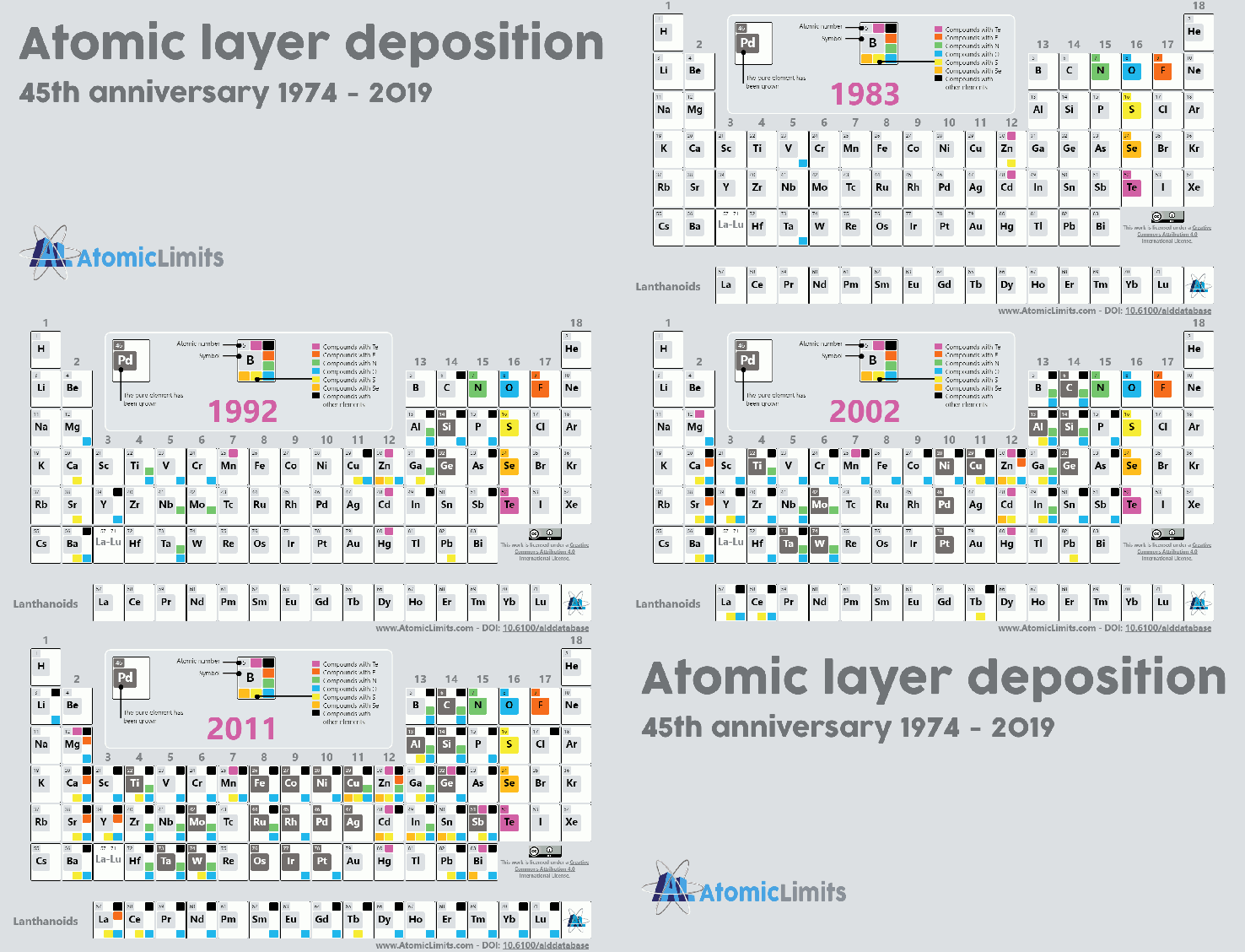
Atomic layer deposition (ALD) has become a very popular method for the preparation of (ultra)thin films over the last two decades, yet it has a rich history which goes back many more years. It is well known that the first patent on ALD was applied for in 1974 [1]. The priority date was November 29, 1974 – so this week we have its official 45th anniversary! A good reason to share an ALD timeline and animated version of the ALD periodic table with you, as you will find below!
Tuomo Suntola and Jorma Antson were listed as inventors on this patent. Tuoma Suntola has been praised extensively for the invention. Its importance was last year also recognized when Tuoma Suntola received The International Millennium Technology Prize 2018. The English title of the first patent was “Method for producing compound thin films” while the method became first known as “Atomic Layer Epitaxy” or “ALE” (note that in the recent years the abbreviation “ALE” is mainly used for Atomic Layer Etching [2]). More information on the invention of ALD by Tuomo Suntola and what it subsequently triggered can be found in an article by Riikka Puurunen published in 2014 when ALD turned 40 years old [3].
There is another article that addresses the history of ALD and especially also its relationship with the American Vacuum Society (AVS) [4]. Through this organization the foundations of the International Conference on ALD were laid, particularly by some active members in its Thin Film Division: Gregory Parsons, Steven George, Stephen Rossnagel and Hyeongtag Jeon. The article [4] – published in the Journal of Vacuum Science and Technology A and 1st authored by Greg Parsons – outlines how ALD developed within the AVS and how it led to the International Conference on ALD which was first organized in Monterey CA in 2001. The article also addresses the fact that the original name for the ALD conference was “ALCVD conference” as Atomic Layer Chemical Vapor Deposition (ALCVD) was a common name for the method at that stage of time. Yet a letter from a tool vendor (from the company ASM) put a stop to this as the company stated that the “ALCVD Conference” name would infringe on their copyright on “ALCVD”. This is how it happened that we talk about ALD now.
The same article also reports on the work on “Molecular Layering” in Russia in the 60’s. It describes research efforts by Russian professors Aleskovskii and Kolt’sov from the Leningrad Technological Institute on a method that is similar to ALD and that preceded ALD research in Finland. As highlighted by Riikka Puurunen (see e.g. her article Learnings from an Open Science Effort: Virtual Project on the History of ALD) [5] the aforementioned article about the history of ALD and its relationship with the AVS appeared to be not fully accurate or to be incomplete at least. The Virtual Project on the History of ALD that was initiated by Riikka Puurunen and which involved many other volunteers revealed a lot of interesting details about the early days of ALD in Russia. See also the publication in the Journal of Vacuum Science and Technology A that appeared in 2017 and that had no less than 62 authors [6].
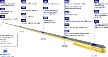
The above demonstrates that when writing about the history of something, one has to be very careful. Important details might easily be missed out and aspects avant la lettre of a certain development can typically not easily be traced back. Moreover, there is a significant risk that a version of a story gets copied over and over again and becomes considered “true” at some point. So taking this into account, it might not be wise to visualize the history of ALD in terms of a simple timeline, yet this is still the thing that I tried to do. I think that a brief graphical representation of the history of ALD can be very insightful and it can also contribute to a better historical perspective of ALD by the community at large. Yet one has to realize that the timeline is oversimplified and always a representation of a personal interpretation. My interpretation of the timeline of ALD is given in the figure below. I also showed this timeline in my plenary presentation at the ALD conference in Bellevue earlier this year.

The timeline is mostly self-explaining and highlights some key “events” over the years which can be found back for a large part in the aforementioned publications. It also shows the developments in terms of (commercial) applications of ALD, the initial (niche) markets but also the subsequent deployment of ALD in high-volume manufacturing in micro/nano-electronics and – since recently – in photovoltaics.
I decided to highlight the fact that the ALD process of Al2O3 – which is now considered the prototypical ALD process – was only reported first in 1989 by Higashi and Fleming [7] but without mentioning something like ALE, ALCVD or ALD in the title or abstract. They just talk about sequential surface (chemical) reactions. In the introduction they do refer to ALE and to the work of Suntola and Antson but for their new Al2O3 process they say in an endnote: “Atomic layer epitaxy is somewhat of a misnomer for this technique as it is difficult to imagine layer by layer growth of an amorphous material.”
The first report on an ALD process in which a plasma is employed has also been highlighted in the timeline. This report by De Keijser and Van Opdorp is from 1991 [8]. Remarkably, the method of plasma-assisted or plasma-enhanced ALD remained subsequently unexplored until the end of the 90s as we highlighted in our first review on plasma-assisted ALD in 2011 [9] (a second, follow-up review was published earlier this year [10]). Even more remarkably – at least for myself – is that the first report came from researchers in Eindhoven and that it is completely independent from our decision to start working (extensively!) on plasma-assisted ALD in Eindhoven about 10 years later (see also the posts about our initial work on ALD here and here).
I have also special memories what the reintroduction of spatial ALD in 2008 concerns. It is labeled as “reintroduction” because the first ALD process of ZnS by Suntola was basically already spatial ALD. Drawings of reactor sketches are also included in the original patent [1]. The reason for the special memories is that I saw the first presentation about (atmospheric pressure) spatial ALD during the 8th International Conference on ALD in Bruges in 2008. Together with Annelies Delabie from IMEC, I happened to be the chair of that conference so I was very much involved. The presentation – given by David Levy from Kodak (see his first publication [11]) – took place in a rather small room on Wednesday afternoon and everyone who saw it was struck with awe. It was the start of an important new development in the field of ALD which has made the method also attractive for applications that really require high throughput processing.
For the year 2012, I have indicated the first pilot production of PERC solar cells containing Al2O3 as back side passivation layer. This is also linked to our research at the TU/e but it also marks the start of a very important new industrial application of ALD in high-volume manufacturing. After less than a decade of research (you can read about it in our earlier blogs here and here) Al2O3 nanolayers made it in the commercial production of PERC solar cells. The development started with research on ALD of Al2O3 [12] and it also very much triggered the field of (atmospheric pressure) spatial ALD although the first production lines were based on PECVD (plasma-enhanced chemical vapor deposition) tools. Yet, also spatial ALD tools made it into production and at the present time the markets appears to be become dominated soon by batch ALD tools, see our recent blog post. In terms of the number of silicon wafers processed, this will be the largest application of ALD in industry!
The latest landmark in the ALD timeline relates to area-selective deposition (ASD), a field that has gained a lot of interest in the last few years and which in many cases involves – but certainly not solely – ALD. In 2016 the first workshop on ASD was organized and next year we will already have our 5th edition: ASD20 will take place at Stanford University on April 2-3, 2020. More information on area-selective ALD can be found in our initial review in 2014 [13] and a more recent perspective article [14]. You can also find several posts about ASD on this blog, e.g., about the use of area-selective ALD in fully self-aligned vias (FSAVs), a stop motion movie about an area-selective ALD process and several ASD workshop reports (2016, 2017 and 2019.
Finally, to wrap this blog post up, I would like to come back again to the 45th anniversary of ALD. Obviously, one thing that has happened over the years and that has really progressed the method and its applications, is the development of a huge number of ALD processes for a very large set – and still growing number – of materials. The growing number of materials that have been prepared by ALD can be visualized using the ALD periodic table that we turned into an online ALD database. See the animated version of the periodic table below and feel free to share and use it!
P.S. Please keep uploading your new ALD processes to the database. Many of you have already done so, thanks for making this a community effort!

References
[1] T. Suntola and J. Antson, patent FIN 52359 (29 November 1974); corresponds to U.S. patent 4 058 430 (25 November 1975).
[2] Overview of atomic layer etching in the semiconductor industry, K.J. Kanarik, T. Lill, E.A. Hudson, S. Sriraman, S. Tan, J. Marks, V. Vahedi, and R.A. Gottscho, J. Vac. Sci. Technol. A 33, 020802 (2015).
[3] A short history of atomic layer deposition: Tuomo Suntola’s atomic layer epitaxy, R. L. Puurunen, Chem. Vap. Deposition 20, 332 (2014)
[4] History of Atomic Layer Deposition and its Relationship with the American Vacuum Society, G. N. Parsons, J.W. Elam, S.M. George, S. Haukka, H. Jeon, W.M.M. Kessels, M. Leskelä, P. Poodt, M. Ritala, and S.M. Rossnagel, J. Vac. Sci. Technol. A 31, 050818 (2013).
[5] Learnings from an Open Science Effort: Virtual Project on the History of ALD, R.L. Puurunen, ECS Trans. 86, 3 (2018).
[6] Recommended reading list of early publications on atomic layer deposition—Outcome of the “Virtual Project on the History of ALD”, E. Ahvenniemi et al., J. Vac. Sci. Technol. A 35, 010801 (2017).
[7] Sequential surface chemical reaction limited growth of high quality Al2O3 dielectrics, G.S. Higashi and C.G. Fleming, Appl. Phys. Lett. 55, 1963 (1989).
[8] Atomic layer epitaxy of gallium arsenide with the use of atomic hydrogen, M. De Keijser and C. Van Opdorp, Appl. Phys. Lett. 58, 1187 (1991).
[9] Plasma-assisted Atomic Layer Deposition: Basics, Opportunities and challenges, H. B. Profijt, S. E. Potts, M. C. M. van de Sanden, and W.M.M. Kessels, J. Vac. Sci. Technol. A. 29, 050801-1 (2011).
[10] Status and prospects of plasma-assisted atomic layer deposition, H.C.M. Knoops, T. Faraz, K. Arts, and W.M.M. Kessels, J. Vac. Sci. Technol. A 37, 030902 (2019).
[11] Stable ZnO thin film transistors by fast open air atomic layer deposition, D.H. Levy, D. Freeman, S.F. Nelson, P.J. Cowdery-Corvan, and L.M. Irving, Appl. Phys. Lett. 92, 192101 (2008).
[12] Status and prospects of Al2O3-based surface passivation schemes for silicon solar cells, G. Dingemans and, W.M.M. Kessels, J. Vac. Sci. Technol. A 30, 040802 (2012).
[13] The use of atomic layer deposition in advanced nanopattering, A.J.M. Mackus, A.A. Bol and W.M.M. Kessels, Nanoscale 6, 10941 (2014).
[14] From the bottom-up: towards area-selective atomic layer deposition with high selectivity, A.J.M. Mackus, M. Merkx, and W.M.M. Kessels, Chem. Mater. 31, 2 (2019).


1 Comment